Crackle Inverter : Speculative Circuit Design #
Ji Youn Kang
Inverter (NOT gate) #
An inverter, or NOT gate, is a fundamental component in digital circuits, specifically designed to manipulate input and output logic level voltages, representing binary bits of 0 and 1. These binary values are depicted through voltage signals in relation to ground within the circuit. The functionality of an inverter extends to its ability to manage currents in two primary ways: sourcing and sinking. Sourcing current involves connecting the output terminal to the integrated circuit’s (IC) power source, typically referred to as Vcc. Conversely, sinking current entails grounding the output terminal, often labeled as Vss, thereby completing the circuit and enabling the flow of electricity in a manner that supports the intended logic operations.
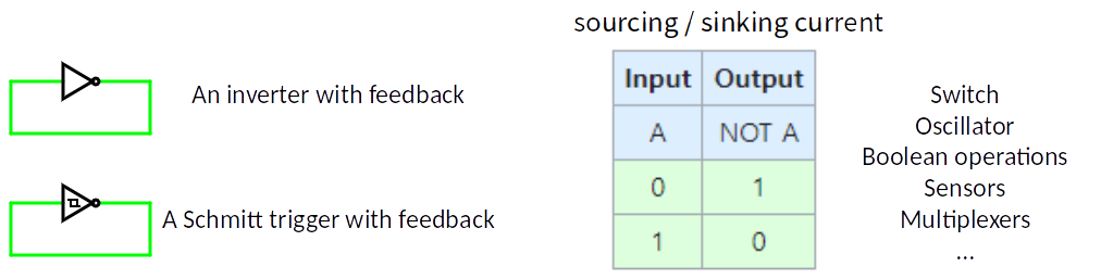
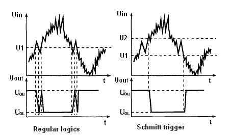
A Schmitt trigger is a specialized form of inverter that incorporates hysteresis, a property that allows the device to react differently depending on whether the input signal is increasing or decreasing. This is achieved through positive feedback, creating a scenario where the output switches to high only when the input exceeds a certain upper threshold and switches back to low only when the input falls below a lower threshold. This dual-threshold mechanism ensures that the output remains stable when the input voltage lies between these two levels, effectively reducing the impact of noise caused by ambiguous voltage levels. By utilizing hysteresis in this way, the Schmitt trigger provides a more reliable solution for oscillator designs, enhancing stability and precision by guarding against unwanted signal variations.
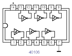
The 4049 CMOS Inverter, unlike the Schmitt trigger, lacks the hysteresis feature. This absence means it tends to generate more noise in its output and can achieve faster frequencies with the same configuration. This characteristic makes designing simple square wave oscillators, akin to those easily created with a 40106 circuit, more challenging with a 4049 CMOS Inverter. This complexity is further accentuated by the fact that each input on the 4049 is designed to either source or sink current. Without hysteresis to provide a buffer against noise and stabilize transitions between high and low states, the precise control of oscillation becomes a more delicate and intricate task, highlighting the distinctive operational differences and design considerations between these two types of inverters.
In theory, an inverter should oscillate correctly, with the oscillation frequency determined by the formula 1/RC×t, where
- R is the resistor value,
- C is the capacitor value, and
- t is the propagation delay time.
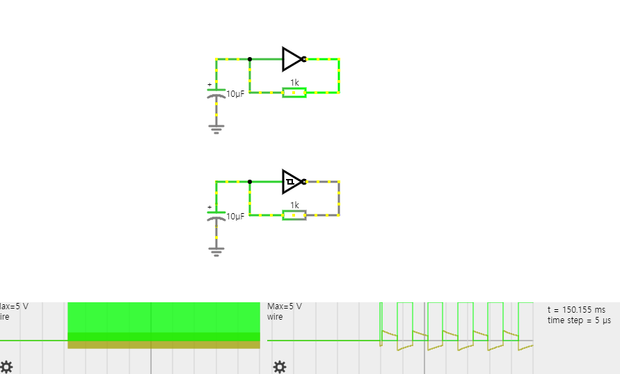
A popular oscillator design is illustrated below; however, this design has a notable flaw: it may not oscillate under certain conditions. This phenomenon can be demonstrated by reducing the capacitor value (C) to zero, which cannot oscillate. This scenario indicates that there exists a critical capacitor value (C1) below which the network fails to oscillate. In practical applications, if a two-gate circuit does oscillate, its frequency is approximately 1/(2.2×C×R2). For more reliable performance, it is recommended to consider alternative designs as outlined in the application note. An oscillator built with a single Schmitt-trigger inverter would oscillate at a frequency of approximately 0.8/(R×C), offering a more predictable and stable output. In the context of my design, such a risk is taken as the final design is not aimed to create stable oscillator but rather an unstable one.
In order to make a stable square wave oscillator with the 4049 IC chip, it should be with another inverter as in the photo below, and even better with three inverters.
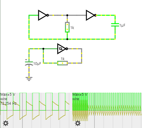
Then I experimented with combinations of inverters. This was rather an improvised version of combining three sets of two inverters in such a way that they ‘collide’ with each other.
A mistake found! A critical oversight was identified in the initial design involving the connection of an audio jack to the output of an inverter. The issue arises because when the audio jack is plugged in, the capacitor fails to charge adequately due to the current being diverted into the jack. To address this problem, an operational amplifier (op-amp) has been incorporated into the design. The inclusion of the op-amp resolves the charging issue by isolating the capacitor’s charging path from the direct influence of the connected audio jack. This adjustment ensures that the capacitor charges as intended, maintaining the circuit’s functionality. The details and implications of introducing an op-amp into the circuit design will be elaborated upon in the next session. The revised final design of the circuit, which includes this critical modification, will be presented accordingly.
Experiment #
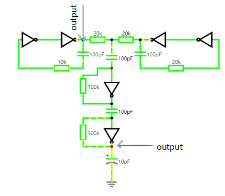
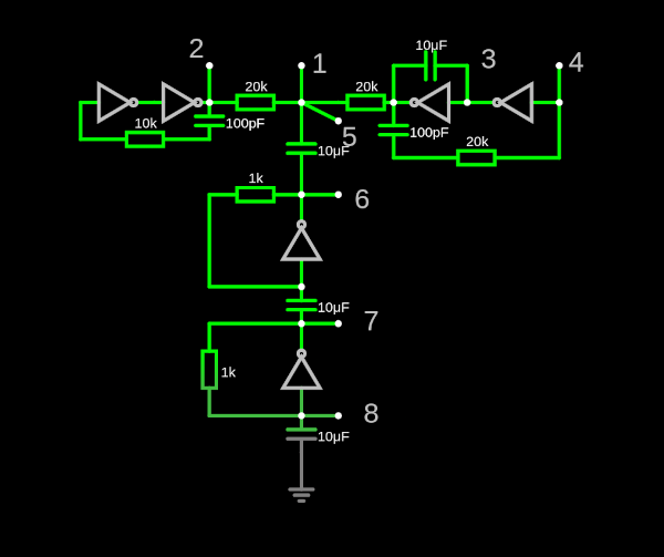
- No.2 from the schematics as an output
- No.5 from the schematics as an output
References #
- P. Horowits, W. Hill, 1980, “The Art of Electronics,” Cambridge University Press
- T.R. Kuphaldt, 2000-2014, “Lessons in Electric Circuits Vo. IV – DIGITAL,” Open Book Project collection
- A. Carlson, G. Hannauer, T. Carey and P. J. Holsberg, 1967, “EAI Handbook of Analog Computation”
- A. Agarwal, J.H. Lang, 2005, “Foundations of Analog and Digital Electronic Circuits,” Morgan Kaufmann Publishers
- The engineering Staff of Analog Devices, INC, 1976, “Nonlinear circuits handbook – designing with analog function modules and IC’s” Analog Devices, INC